LumArray's Technologies

A hallmark of LumArray’s development efforts, as well as our micro/nano-fabrication services, is maskless lithography. For customized, modest-volume micro- and nano-fabrication, maskless lithography has numerous advantages over photomask-based lithography. Also, when patterned areas exceed the 22 x 30 mm field size of indusial scanners, maskless lithography is the only reasonable alternative.

In addition to our maskless lithography technologies, LumArray has a suite of processing and analytical tools, including etching tools, optical microscopy, electron microscopy, surface metrology and an in-house-invented interferometric tool that checks the short-range and long-range spatial-phase coherence of patterns created by our maskless lithography tools.

Zone-Plate Array Lithography

LumArray’s ZP-150 maskless photolithography system is based on zone-plate-array lithography (ZPAL), a technology invented at MIT’s NanoStructures Lab. The following graphics illustrate ZPAL and show LumArray’s ZP-150 within its environmental enclosure.

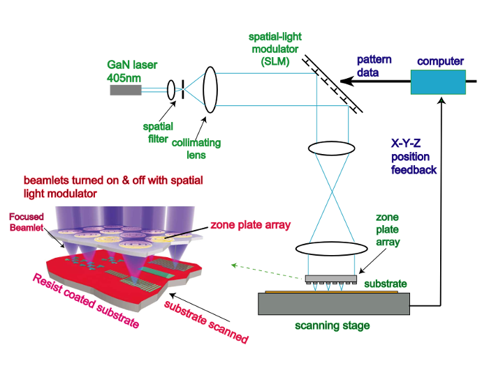
Schematic of the operating principle of zone-plate-array lithography (ZPAL).

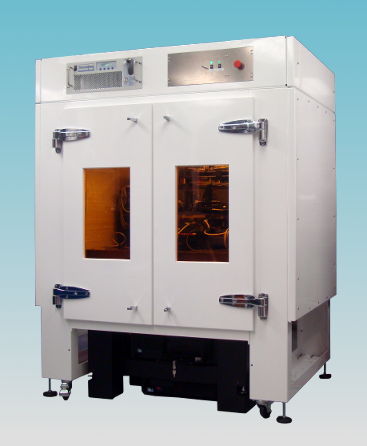
Photo of LumArray’s ZP-150 system within its environmental enclosure.

The ZP-150 achieves high throughput for patterns of arbitrary geometry, covering up to a full wafer area, using an array of up to 1000 independently programmed diffractive-optical microlenses. An example of such arbitrary patterning is the hologram shown under Micro- & Nanofabrication services.

The ZP-150 achieves nanometer-level accuracy in the placement of pattern elements by combining a high-stability mechanical design with correction in software for systematic placement errors. In brief, placement errors are measured using a proprietary phase-sensitive interferometry that enables the ZP-150 to achieve ~10 nm pattern-placement accuracy over full-wafer fields, rivalling state-of-the-art e-beam photomask writers. This capability is important in diffractive-optical applications such as precision x-ray spectroscopy. Photonic applications based on preserving temporal coherence likewise require the long-range spatial-phase coherence the ZP-150 provides.

Currently, the ZP-150 utilizes microlenses with numerical apertures (NA) of 0.55 and a source of 405 nm wavelength, limiting linewidth resolution to ~300 nm. As in any photolithography system, resolution is improved with higher NA and/or shorter wavelength. Using microlenses of 0.85 NA, linewidths of 122 nm were demonstrated previously. LumArray is currently investigating optimal methods of fabricating diffractive-optical microlens arrays of higher NA and higher focal efficiency.

Mach-Zehnder Interference Lithography

Another form of maskless lithography at LumArray is Mach-Zehnder Interference Lithography (IL). It’s suitable only for exposing periodic gratings and grids. Our system features fringe locking, spatial periods down to 180 nm and areal coverage up to 150 mm diameter.

Achromatic Interference Lithography (AIL)

LumArray’s deep-UV Achromatic Interference Lithography (AIL) system was developed during the 1990’s at MIT’s Nanostructures Laboratory. It exposes gratings and grids of 100 nm spatial period over areas up to 50 x 50 mm. (See examples under Micro- & Nanofabrication Services.) Larger areas can be achieved by step and repeat exposures, but spatial-phase coherence between stepped fields is not guaranteed.

Scanning-Electron-Beam Lithography (SEBL)

LumArray utilizes its Raith 150 scanning-electron-beam lithography (SEBL) system when pattern resolution requirements are finer than can be achieved with the ZP-150 system. Examples include the fabrication of Fresnel zone plates, shown under Micro- & Nanofabrication Services.