|
In semiconductor lithography, glass masks are illuminated
with deep UV laser light and their image is reduced through a lens onto
the substrate to define circuitry. As feature sizes are pushed toward
100 nm, lithography is becoming increasingly costly and difficult, and
may soon limit the industry juggernaut.
A new technology developed at the NanoStructures Laboratory at M.I.T.
is showing great promise. The new scheme, called zone-plate-array
lithography (ZPAL) is made
possible by inexpensive, high-speed computation and micromechanics.
ZPAL replaces the "printing press" of traditional lithography with a
technology more akin to that of a "laser printer".
Instead of a single, massive lens, a large array of
microfabricated diffractive optical elements (Fresnel-zone-plate
lenses) is used, with each element focusing a beam of light onto the
substrate. A computer-controlled array of micromechanical elements
turns the light to each lens on or off as the stage is scanned under
the array, thereby printing the desired pattern in a dot-matrix
fashion. No mask is required, enabling designers to rapidly change
circuit designs. A schematic of ZPAL is shown in Figure 1.
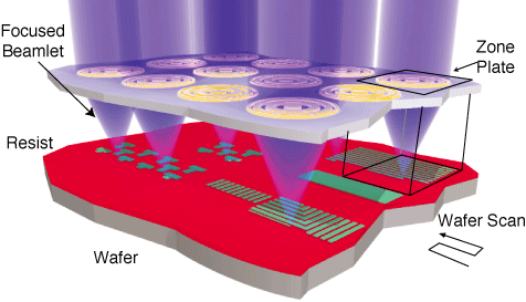
Figure 1:
Schematic of zone-plate-array lithography (ZPAL). An array of Fresnel
zone plates focuses radiation beamlets onto a substrate. The individual
beamlets are turned on and off by upstream micromechanics as the
substrate is scanned under the array. In this way, patterns of
arbitrary geometry can be created in a dot-matrix fashion. The minimum
linewidth is equal to the minimum width of the outermost zone of the
zone plates
This technology
is capable of printing patterns of complex geometry as illustrated by
the scanning-electron micrograph of the seal of MIT that was printed
using the MIT-ZPAL system at a wavelength of 400nm. Note that features
as small as 140nm was resolved.
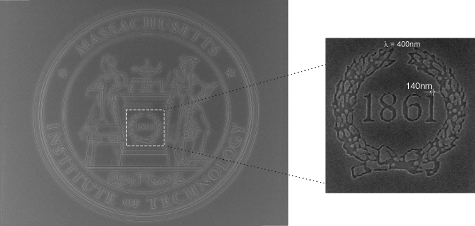
Figure 2:
Scanning-electron micrographs of the seal of MIT.
ZPAL leverages advances in nanofabrication,
micromechanics,
laser-controlled stages, and high-speed, low-cost computation to create
a new form of lithography. We are developing ZPAL at UV and deep UV
(DUV) wavelengths, although extensions to EUV and X-ray wavelengths are
possible. With the goal of proving both the technical merit and the
potential commercial viability of ZPAL we are currently building a
prototype system that will be used for quick-turn-around, maskless
patterning for a number of research applications, from MEMS to
microphotonics.
Figure 3 presents some of the high quality lithographic
patterns that the M.I.T. ZPAL system produces. All patterns show good
fidelity, low edge roughness, and the ability to pattern very dense
features down to the minimum spot size. A large number of patterns were
exposed with the system, including 2D photonic bandgap structures (Fig
3(d-e)), microcomb structures (Fig 3(f)), waveguides (Fig 3(g)), zone
plates (Fig 3(h)), and a number of lithographic test patterns (Fig
3(a-c)).
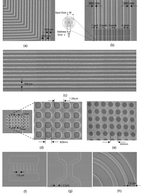
Figure 3.
Scanning electron micrographs of patterns exposed at MIT's
continuous-scan UV-ZPAL system. (a) Dense nested Ls, (b) single-pixel
lines with different spacing between lines, (c) small section of a 81
mm-long, 600nm-period grating, (d) 2D photonic bandgap structures with
1.29 mm period, (e) 2D photonic bandgap structures with 600 nm period,
(f) microcomb structure for MEMS, (g) curved waveguides, (h) portion of
a zone plate. All exposures presented in Figure 2 employed a 25 mW GaN
laser diode operating at 400 nm wavelength. For these experiments no
multiplexing device was used, i.e., all zone plates in the array wrote
the same pattern simultaneously.

Figure 4: (a)
Scanning-electron micrographs of dense line/space patterns produced
with MIT's UV (l=400 nm)
ZPAL system. The minimum feature size of an optical projection system
can be described as Wmin=k1*l/NA. In this case the smallest linewidth
is 135 nm, the numerical aperture (NA) of the zone plates was 0.85,
corresponding to a k1 factor of 0.287. (b) Scanning-electron micrograph
of a non-periodic pattern with smallest feature-width of 122nm. By
using 193nm light under water immersion, we expect to be able to print
39 nm features.
Because zone plates are diffractive optical elements, ZPAL
can operate at EUV wavelengths (13.4 nm) or even in the soft x-ray
regime (l~1-5 nm). EUV or soft x-ray ZPAL should enable us to achieve
feature sizes of about 20 nanometers.
|