ZP-150
Affordable high-throughput, high-resolution, maskless photolithographic patterning for research, product development and low-volume or customized manufacturing.
| ZP-150 Performance Specifications | |
|---|---|
| Minimum Feature Size: | 200 nm with 0.85 NA lens array 600 nm with 0.30 NA lens array |
| Number of Parallel Beams: | 1000 |
| Dose Uniformity: | <1% across all 1000 beams |
| Writing Speed: |
1.7 mm2/sec, 100 mm2/min @ NA=0.85, 200 nm features process-dependent; increases in throughput are possible at lower resolution |
| Grayscale: | Optimized 8-bit grayscale in every pixel |
| Design Grid: | 5nm |
| Positioning Resolution: | 1.2nm |
| Maximum Pattern Area: | 150mm x150mm |
| Alignment / Overlay: | <50nm |
| Field Size: | Up to 150mm x 150 mm (stage travel limit) |
| Exposure Wavelength: | 405nm (I-line, G-line compatible) |
| Environmental Enclosure: | Particulates to ISO Class 5, temperature to 0.1°C |
| Control Software: | LithZone platform-independent, remote access web app |
| Layout Format: | GDS II / OASIS |
| Computation: | Nvidia GPU Server, 6TeraFlops with 4608 parallel cores |
| File Archive: | 30 TB PCI-express storage server |
| Physical Aspects & Facilitation | |
|---|---|
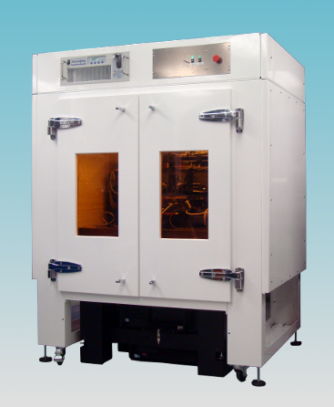
| Footprint: | ZP-150: 60” wide x 40” deep x 72” high Electronics Rack: 24” wide x 30” deep x 48” high Clearance: Recommended minimum clearance 36” behind the tool, 48” in Total: Approximately 10’ x 12’ (including machine access and desk) |
| Weight: | ZP-150: ~2500 lb. Electronics Rack: ~400 lb. |
| Electrical: | ZP150: 30 Amp, 208 to 240 VAC |
| Compressed Air: | Compressed dry air to ISO Class 4 or better (15 micron filter, 37.4˚F dew point, 1 mg/m3 oil vapor). We strongly recommend the use of an oil-less air compressor. Supply requirements: 15 scfh @ 100 psi |
| Vacuum: | Vacuum to 20” Hg minimum |
| Environment: | The ZP-150 includes an environmental enclosure for critical areas of the tool controlled to ISO Class 4-5 for particulates, and temperature stabilized to 0.1°C. We recommend the installation environment be clean to better than ISO Class 7 (Fed Std. 209E Class 10,000) with temperature stability better than 5°C. |
| Vibration: | Recommended environmental vibration criterion better than VC-C (500 micro-in/sec). Installation on ground-level concrete or other solid flooring recommended. Pneumatic isolation is integrated in the ZP-150 making floor-level isolation unnecessary. |
| Facility Access: | All components of the ZP-150 are fully castered to simplify movement and location in the lab. If necessary, all components will fit through a single 84”x36” door opening although we recommend double-wide door access. |